In Part 1, I discussed test jigs that were passive devices (unless you consider a light bulb and a power cord active devices). Now, I’ll present some more active electronics-based devices.
In Figure 1, here’s a purchased PC board module based on the Diodes Inc. PAM8403 stereo class-D power amplifier, 2 watts per channel. I was working on a project that used several of these prefabricated ‘8403 boards, and I needed a way to check their outputs with a ‘scope to make sure they were not “clipping” (in analog-speak) or running out of headroom. I planned on building a monitoring device to easily and quickly run tests on multiple devices. But first, I decided to set up one board all by itself so I could figure out how to run my test procedure. To make working with this one board a bit easier, I mounted it on a larger piece of perfboard. I added a few 0.1″ pin connectors to make it easier to connect power, signal inputs, and speaker outputs.
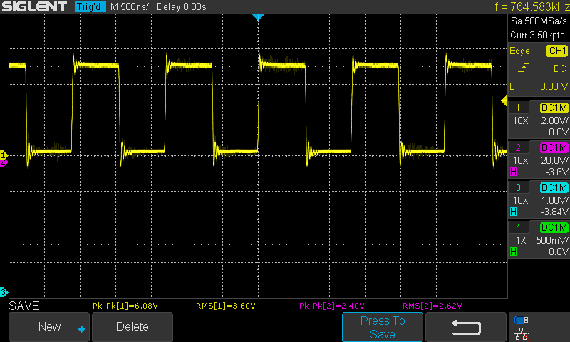
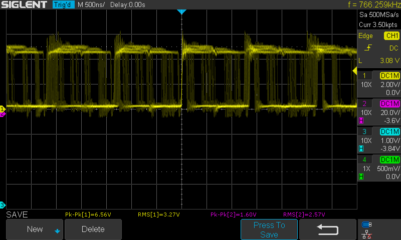
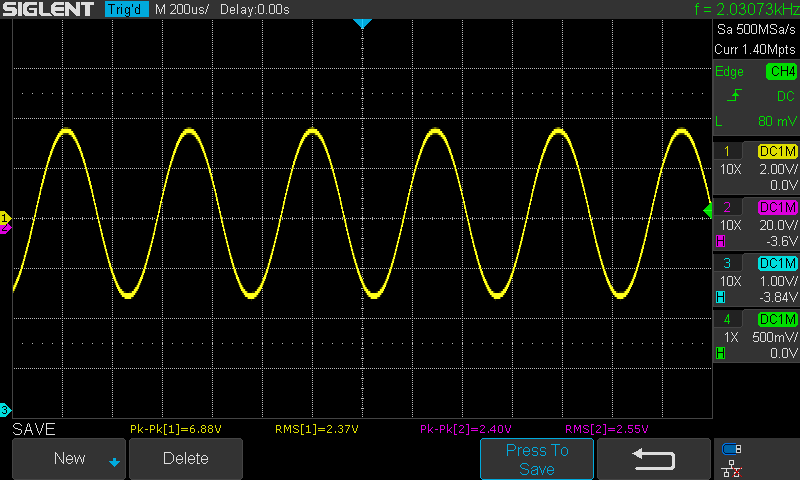
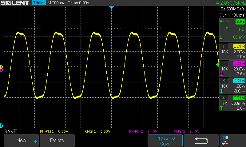
Since the output from each amplifier is a series of pulse-width modulated rectangular waves (see Figure 2 and Figure 3), you can’t simply put a ‘scope probe on an output pin and see if it’s clipping.
Instead of trying to evaluate the amplifier’s performance by scoping its outputs, you need to perform the same action that the speaker does – you need to integrate the applied waveform (i.e., low-pass filter it) and look at that with the scope.
This brings us to the actual test jig that I built. Recall that I would be testing multiple devices; I needed a way to quickly evaluate the ‘8403 modules that were piggy-backed onto my PC board. The class-D amplifier output is a type of differential output. On one amplifier output, there is a stream of rectangular waves of varying duty cycle from approximately zero to 100% (50% at idle). On the other amplifier output, there is a matching synchronized stream varying from approximately 100% to zero.
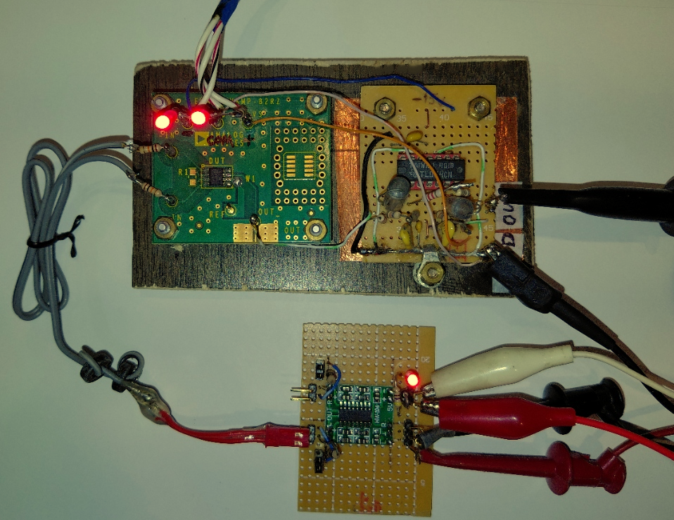
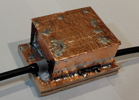
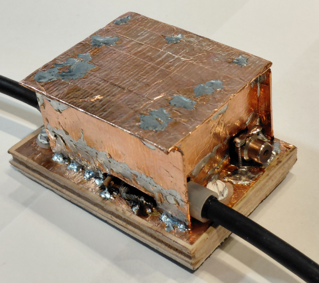
The load (the speaker) is tied across the two outputs rather than from output to circuit common or ground. This is commonly referred to as a bridge-tied load or BTL. I needed a way to monitor the amplifier outputs in differential mode and then produce the analog equivalent through integration. In Figure 4, here’s what I built.
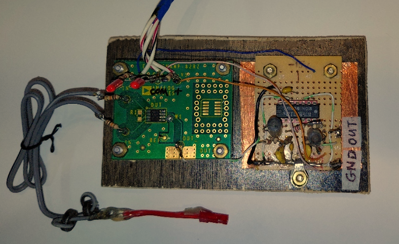
There are two boards here. One is a PC board, and the other is a perfboard. The perfboard contains a bit of circuitry: a quad op amp and a handful of resistors and capacitors. I mounted both boards on a piece of scrap plywood using standoffs and 4-40 hardware. I also added a copper foil ground plane beneath the perfboard. The use of scrap lumber to build test jigs is a favorite method of mine – it’s inexpensive and can easily accommodate various amounts of circuitry. It’s not perfectly shielded, but that’s not always necessary.
The PC board is an Instrumentation Amplifier Eval board I acquired during my time working for Analog Devices. I populated it with an AD8421 and powered it from ±15 VDC. I equipped the (true) differential input with a connector to match the pins on the ‘8403 amplifier boards I was building. I also added some small ferrite toroids to reduce the high-frequency content. The perf-board is a four-pole active low-pass filter with a corner frequency of 10 kHz and a pass-band gain of unity (1 V/V). Figure 5 shows the set up in use. Figure 6 and Figure 7 show the ‘scope output with a 2 kHz signal input, below and above the level where clipping and distortion start.
This setup made it easy to evaluate my devices. I could ensure they were all built correctly with no defective components.
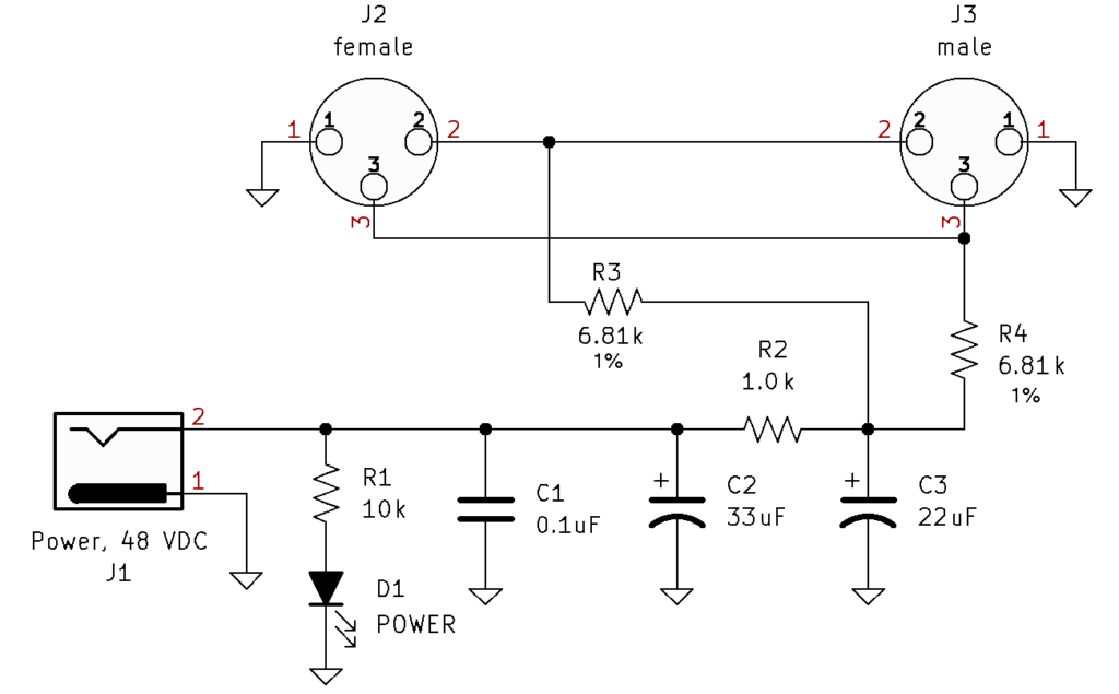
I built another piece of audio equipment to make it easy to test microphones that needed phantom power. A phantom power supply provides (usually) +48 VDC to microphones that have built-in preamplifiers. The term phantom and the use of 48 VDC derive from the early days of telephony and tube preamplifiers. A low-power tube amplifier’s plate circuitry could be operated from 48 V effectively. Phantom circuitry allows a second circuit (the power, in this case) to be overlaid on the primary circuit (the audio).
With a balanced audio line – the kind that typically uses XLR connectors on the cable – there are two wires carrying the audio inside the grounded shield. The signal on one wire is 180° out of phase with the signal on the other. Stated another way, the audio is sent differentially through the cable. The 48 VDC is coupled onto both these wires through two almost identical resistors (1% tolerance) sized at a few thousand ohms. This means the DC is sent via common mode (with respect to ground) on the balanced audio line. The resistors don’t appreciably load the audio from the microphone, which typically has a source impedance of perhaps 50Ω to 150Ω. The circuit I built to provide the phantom power is shown in the schematic in Figure 8. Power comes from a 48 VDC wall-wart plugged into J1. I added a network of one more resistor and three capacitors to minimize the power supply ripple.
The apparatus is shown in Figure 9, again, built on a scrap of plywood with some copper foil added as a low impedance ground plane. The left cable goes to the female XLR connector (J2); the right cable goes to the male XLR connector (J3). The power cable comes in at the top and plugs into J1.
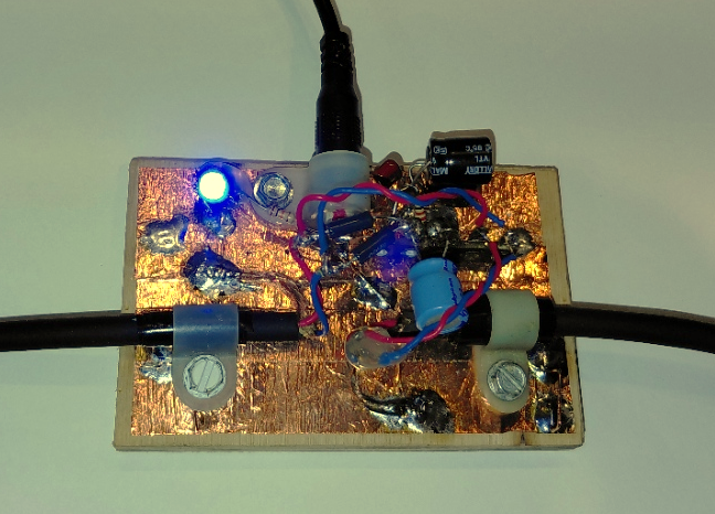
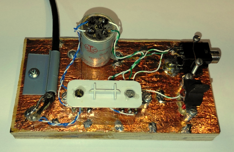
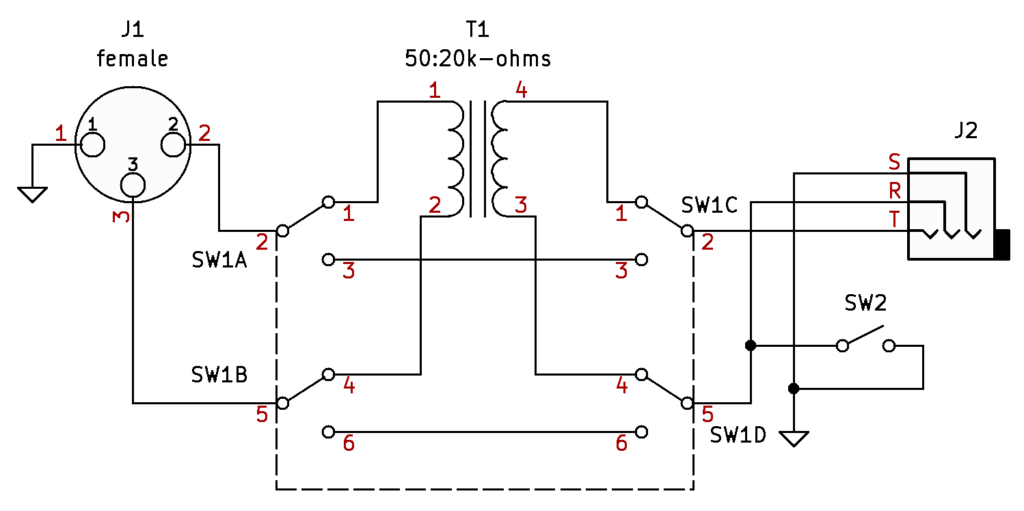
Another useful jig to have for audio work is a microphone matching/isolating transformer, again built on plywood and using parts I had available to control costs. See Figure 10. The microphone plugs into the cable that comes in from the top of the picture (via J1 as seen in Figure 12). There is a lo-Z to hi-Z transformer mounted upright on the board, followed by a ¼” audio connector. This connector is a two-circuit connector, sometimes referred to as a stereo audio jack or a T-R-S connector. T-R-S refers to tip-ring-sleeve, the three electrically isolated sections of the jack and corresponding plug. As before, the terminology derives from telephony technology.
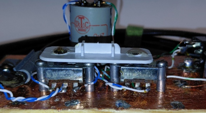
This jig is set up as balanced in, balanced out. Occasionally, I used this jig simply as an adapter to convert an XLR connector to a ¼”audio connector with no need for an impedance transformation. To completely bypass the transformer, I needed a 4PDT switch. I had an abundance of DPDT slide switches, so I used two and ganged them together as seen in more detail in Figure 11.
Since I sometimes plugged the hi-Z side directly into an amplifier that was configured as single-ended, I added a switch (SW2) to ground the ring circuit. Refer to Figure 12 to see how switches SW1 and SW2 function.
As a variation of the previous transformer jig, and to address my concerns regarding the pickup of stray electrical fields (RF and audio frequency), I built the test jig seen in Figure 13. Electrically, much like the version in Figures 10 to 12, but without the switches, I built this to minimize extraneous pickup. It is configured as Lo-Z balanced in and Hi-Z unbalanced out. To provide the needed shielding and to minimize cost, I wrapped sections of cardboard (from the back of a pad of paper) with adhesive-backed copper tape and soldered these panels together. Not surprisingly, it’s fabricated on a scrap of plywood.
In Figure 14, note the added RCA pin jack. I installed that to provide an easy ‘scope test point to monitor the signal going to my amplifier while still maintaining my shielding.
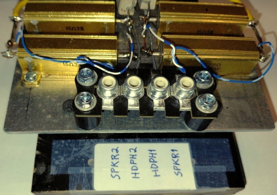
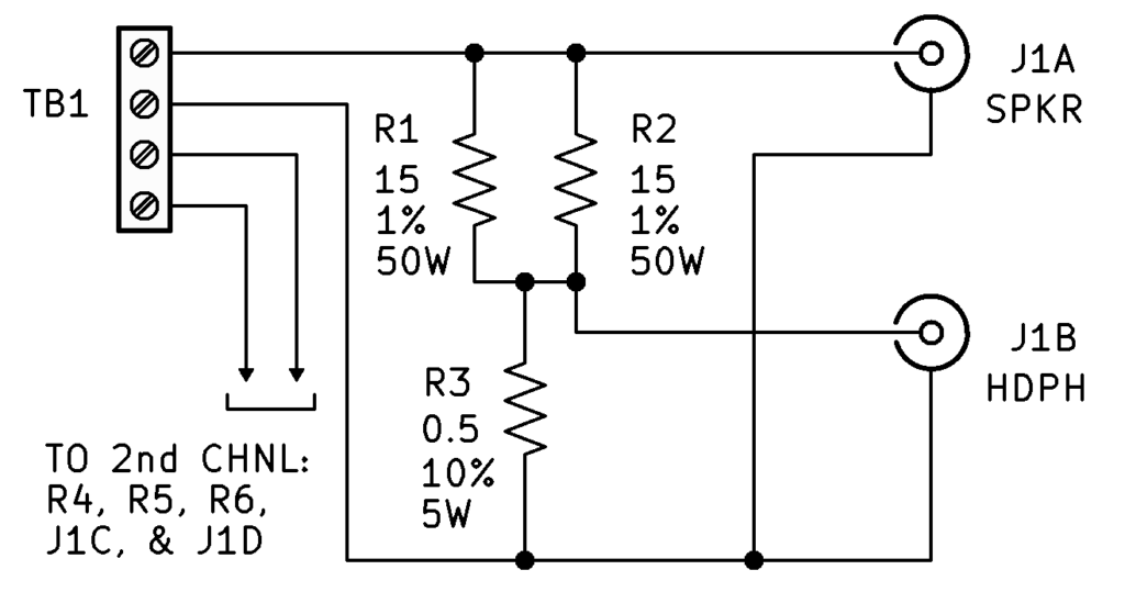
Speaking of amplifiers, if you are testing high-power units and don’t want to blast your eardrums into oblivion, you need to operate the amp into a dummy load. Typical loads are made of 4Ω, 8Ω, or 16Ω resistors. I built a simple one that I can use as either a stereo 8Ω load or, with suitable jumpers, a mono 4Ω or 16Ω load. I happened to have four 15Ω, 1%, 50W power resistors. With two in parallel, I had a 7.5 Ω, 100W resistor – close, but no cigar. I also had a couple of 0.5Ω, 10%, 5W resistors on hand. With one of those in series with each 7.5Ω, I had my dual 8Ω dummy load resistors. An additional advantage of the 7.5Ω+0.5Ω arrangement: It provides a convenient voltage divider point that can drive headphones without damage – it’s functioning as a 1:16 voltage divider.
Referring to Figures 15 and 16, the input is applied via the left two screw terminals on the barrier block. The amplifier’s output can be monitored via a ‘scope at the far-left RCA jack or via headphones at the second from the left RCA jack. The second or right-hand channel is a mirror image of the first with respect to the connections.
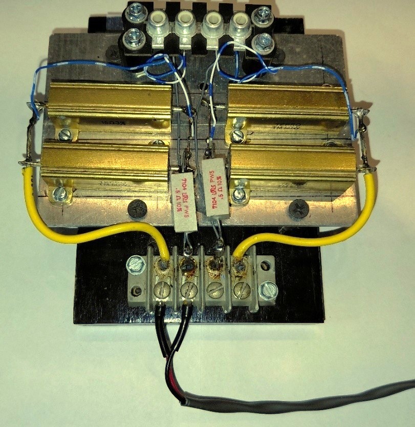
While the power resistors have a rating of 100W, realistically, that presumes an infinitely large heat sink. Since I don’t have one of those available in my lab, I used a substantially smaller than infinity aluminum plate. Heat sink size and thermal conductivity between the resistors and the heat sink; and the heat sink and the ambient air surrounding the heat sink; and the temperature of the ambient air affect how hot the resistors will get versus the power being dissipated in them. So that smaller size heat sink means the resistors’ power rating must be derated from 100W, but the rating is still big enough for most of my testing, especially with short duty cycles of applied power. The schematic of the dummy load is shown in Figure 17.
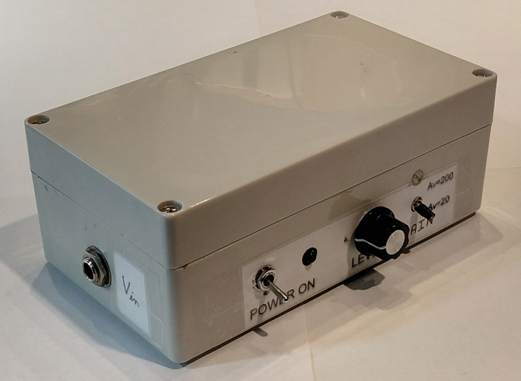
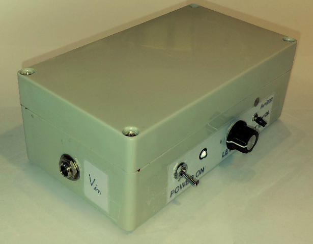
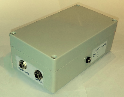
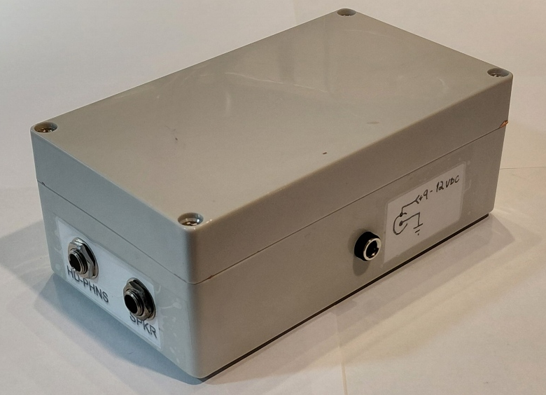
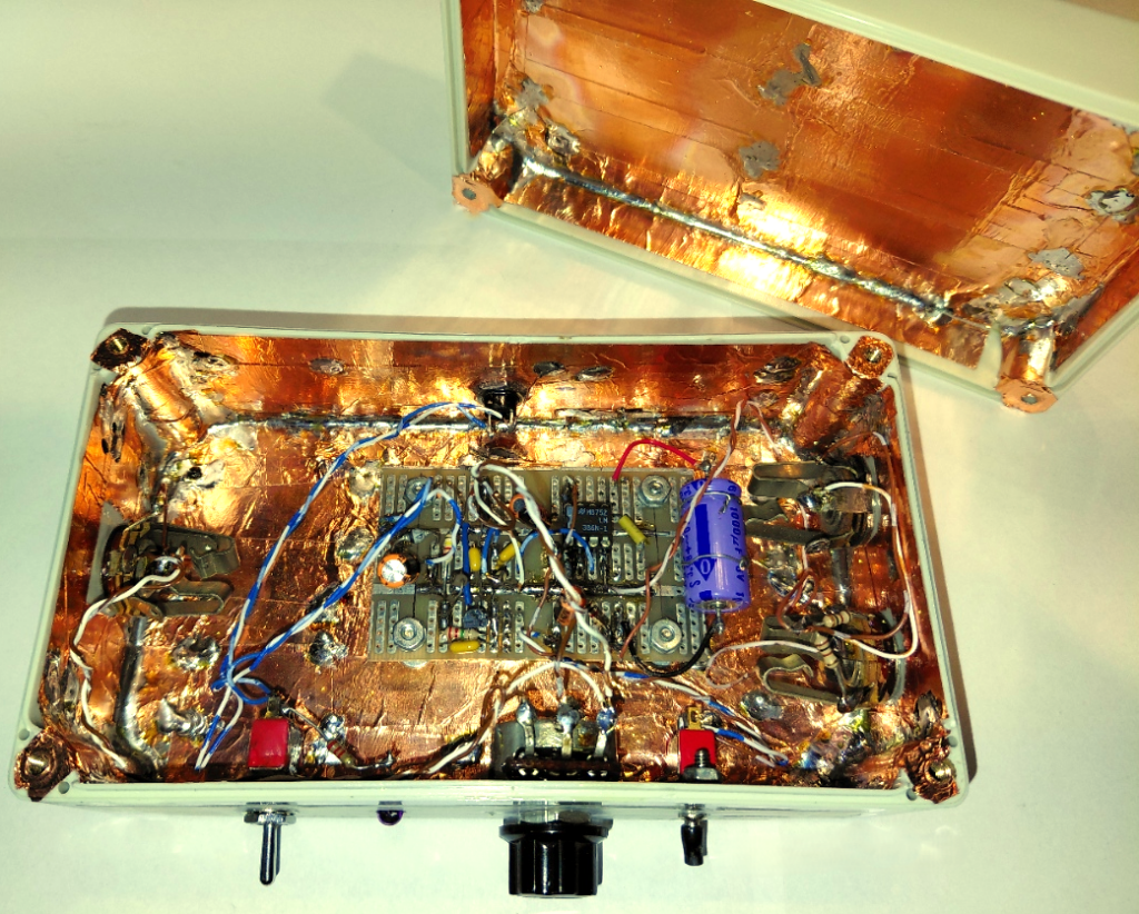
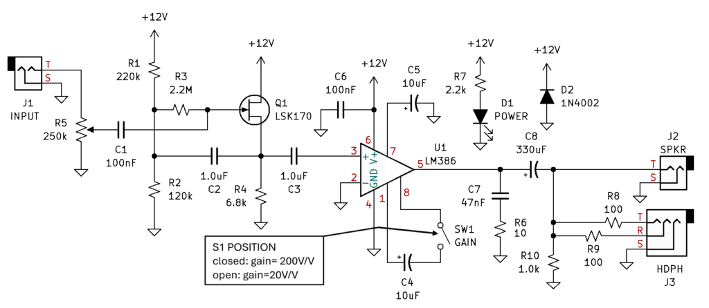
Also on the topic of amplifiers, sometimes you need to amplify low-level signals (e.g., from a guitar) enough to be useful (i.e., be able to hear them). I built a small headphone amplifier using an LM386. It actually can drive a speaker to a quite usable level. One minor detail that makes it slightly problematic: The typical LM386 circuit has a fairly low input impedance of 50kΩ. To work around this, I added a simple JFET source follower circuit to buffer the input of the LM386. The JFET input is bootstrapped to make the input impedance super high. I built this all up on a perfboard and made provisions for gain switching between 20 V/V and 200 V/V. I also provided a direct output to drive a speaker and a resistively padded output to drive stereo headphones. The completed amplifier is shown in Figures 18, 19, and 20.
The schematic is shown in Figure 21.
Please post suggestions of test jigs and apparatus you’ve constructed for your own specific applications.