This section explores the attributes and features of wave and reflow soldering.
Q: What are the main characteristics of wave versus reflow soldering?
A: Each approach has pros and cons related to production rate, type of components, and potential programs. Each process can be looked at from different perspectives, such as best-fit applications, speed of processing, size of equipment needed, and energy consumption.
Q: What are the attributes of wave soldering?
A: In general, wave soldering is the choice for through-hole components, wires, and connectors soldered to the PC board edge, and boards that are loaded only on a single side. It is a relatively high-speed process with boards moving quickly and uninterrupted through the machine.
In terms of solder-joint quality, it offers even solder deposition. The primary potential defects are “shadowing” or disturbed joints due to wave unevenness or microturbulence, leading to solder skips, flux residue trapping under components, and bridging between leads and pads. Defects can often be manually reworked.
A complete wave-soldering system setup is about 10 meters long and costs about $50,000 to $150,000. It is also energy efficient, with high thermal efficiency as the solder is constantly maintained in a molten phase, with preheating as the other major energy need, while heat recovery reduces energy usage.
Q: What about reflow soldering?
A: It is the only practical option for SMT components. If through-hole components are also needed, they must be soldered by hand or using a carefully modulated wave process as a second step. Reflow is the choice in most cases for high-density boards with small components and for fine pitch components, due to its precise paste deposition, even heating in the oven that avoids thermal gradients and joint inconsistencies, and it can be used in one pass for boards loaded with components on both sides. However, large components and boards usually need customized oven profiles.
Energy costs for a reflow setup are higher than for a wave arrangement. The repeated heating of the oven and paste deposits consumes more energy, while the forced convection ovens consume high power. A typical reflow system requires about 25 linear meters (including optical inspection) and costs between $200,000 and $500,000.
Reflow soldering and defects
Q: What are some common reflow-soldering defects?
A: It’s a long list, as reflow soldering is a highly sophisticated process. The most common ones are:
Solder bridging: Unwanted connections between adjacent pads or leads due to excess solder forming a bridge, seen in Figure 1.
Tombstoning: A component standing upright on one end, resembling a tombstone, as shown in Figure 2, due to uneven soldering or other causes.

Solder Balling: Small, unintended balls of solder forming on the PC board surface as seen in Figure 3, potentially resulting in short circuits.

Head-in-pillow (sometimes called ball-and-socket) defect is a serious BGA (Ball Grid Array) solder-joint failure where the solder ball and paste do reflow but fail to fully join, creating a weak, unreliable connection resembling a head resting on a pillow, seen in Figure 4. It is especially insidious because it is not visible, and the connection may function properly at first but become intermittent in the field. Detecting it requires advanced 2D or even 3D X-ray, which is a complicated and costly analysis.

Each of these problems has many possible root causes, and there is often little consistent one-to-one relationship between cause and effect. Among the many possibilities are Insufficient paste deposit causing poor wetting of the joint to be soldered, reflow voids due to poor paste application or profiles, temperature profile errors, poor component pick-and-place placement, to cite a few; it’s a long list of possibilities.
Reflow soldering and through-hole components
Q: Can reflow soldering be used with through-hole components?
A: Sometimes it can be done with special steps using pin-in-paste (PIP) application, but only in situations where the through-hole component size, thermal mass, and resistance to high temperature are compatible with SMT components. In PIP reflow, the solder paste first fills in the holes on the board. Then, the through-hole component’s pins are plugged into the holes, with some solder paste coming out on the other side of the board. Finally, reflow soldering is implemented to complete soldering.
Generally speaking, reflow soldering works best for SMT assembly, while wave soldering is for THT or DIP assembly. Nevertheless, a circuit board almost never contains just surface-mount devices (SMD) or through-hole components.
For mixed assemblies, SMDs and reflow are normally done first, and then THT components are done using wave soldering, since the temperature required for reflow soldering is much higher than that required for wave soldering. If the sequence of two assemblies is reversed, the solid solder paste will possibly melt again, with well-soldered components suffering from defects or even falling from the board.
From through-hole to SMT components
Q: What are component vendors doing to increase the availability of SMT components that can be reflow soldered?
A: Due to the wide use of reflow technology, vendors introduce nearly all their products in SMT packages when feasible, and devote considerable effort to doing so. Most new ICs are available only in SMT packages.
Some passive and higher-power active devices are only offered in THT versions for technical reasons such as power-handling or regulatory considerations. Nevertheless, vendors are investing effort to try to transform these THT devices into SMD versions.
Q: Can you give examples?
A: Two recent component introductions are noteworthy:
- Vishay Intertechnology recently introduced an SMT version of their through-lead safety resistor (a resistor and fuse as a single device), seen in Figure 5. Although it looks at first as if a simple twist of the existing leads is all that is required to provide an SMT version, developing their AC03-CS Series of axial cemented, leaded wirewound safety resistors actually required much more than that. The reason is that the component must meet multiple stringent safety mandates to be certified for its role as a protection device; even the PC board solder-pad land pattern is unique – a small price to pay for the ability to have an SMT version.
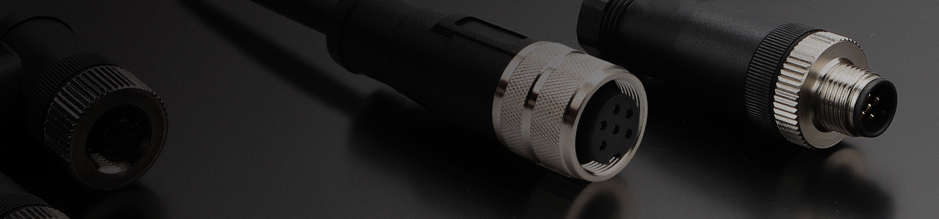
- Connector vendor Weidmüller Group has developed what they call “through-hole reflow” (THR) technology for some connectors, which normally are wave soldered. Their terminal-block connectors for discrete wires do require PCB holes and through-hole mounting for mechanical integrity, as shown in Figure 6, yet can be soldered using a pin-in-paste (PIP) variation and standard reflow process along with other SMT devices on the board. The connectors in this family target PROFINET applications and support Ethernet-compliant data transmission up to 100 Mbit/second.
 Figure 5. (left) This safety resistor with integral fusing was transformed from an existing through-hole device to be surface-mount compatible by clever twisting of its leads, and it meets stringent regulatory mandates associated with the role of this component. (Right) One minor PCB consequence of the change is the pair of T-shaped solder pads recommended by the vendor. (Image: Vishay Intertechnology)

Summary
Wave soldering uses a molten solder “wave” for through-hole technology (THT) components and is well-suited for high-volume production and physically rugged solder joints. Reflow soldering for surface-mount technology (SMT) components melts pre-applied solder paste using hot air, offering precision for complex, high-density boards. Each approach is a sophisticated, complex operation that requires different equipment and process-control sequencing.
References
Printed circuit board, Wikipedia
A Comparison of Reflow Soldering and Wave Soldering, All About Circuits
Wave Soldering vs. Reflow Soldering, Millennium Circuits Limited
What is the difference between wave soldering and reflow soldering?, RAYMING Technology
Comparison between Wave Soldering and Reflow Soldering, PCBCart
Reflow Soldering vs Wave Soldering: Difference and Process, NEXTPCB
Solder Reflow: An In-Depth Guide to the Process and Techniques, Wevolver
Wave soldering, Wikipedia
Reflow Solder Defects, Optima Technology Associates, Inc.
Troubleshooting Reflow Soldering Defects: A Practical Guide for Engineers, ALLPCB
Smarter Temperature Setup for Reflow Oven to Minimize Temperature Variation Among Components, IEEE Transactions on Components, Packaging and Manufacturing Technology
Head-in-Pillow BGA Defects, AIM Solder
Reflow Soldering Process Manual: A Comprehensive Guide From Design To Implementation, Zhejiang Neoden Technology Co., Ltd
Wave and Reflow Soldering, PIEK International Education Centre
AC03-CS Series Axial Cemented, Leaded Wirewound Safety Resistors, Vishay Intertechnology
PCB assembly with THR technology, Weidmüller Group
Related EE World content
Printed Circuit Boards, Part 1: Context and phenolic boards
The basics of FR-4 Printed Circuit Boards
Printed Circuit Boards, Part 3: Vias and multilayer boards
Printed Circuit Boards, Part 4: Beyond FR-4
Why would you use a zero-ohm resistor?
Have you considered resistance soldering? Part 1
Have you considered resistance soldering? Part 2
Step-by-step PCB soldering tips for newbies
What are the different stages of PCB design, testing, and manufacturing?